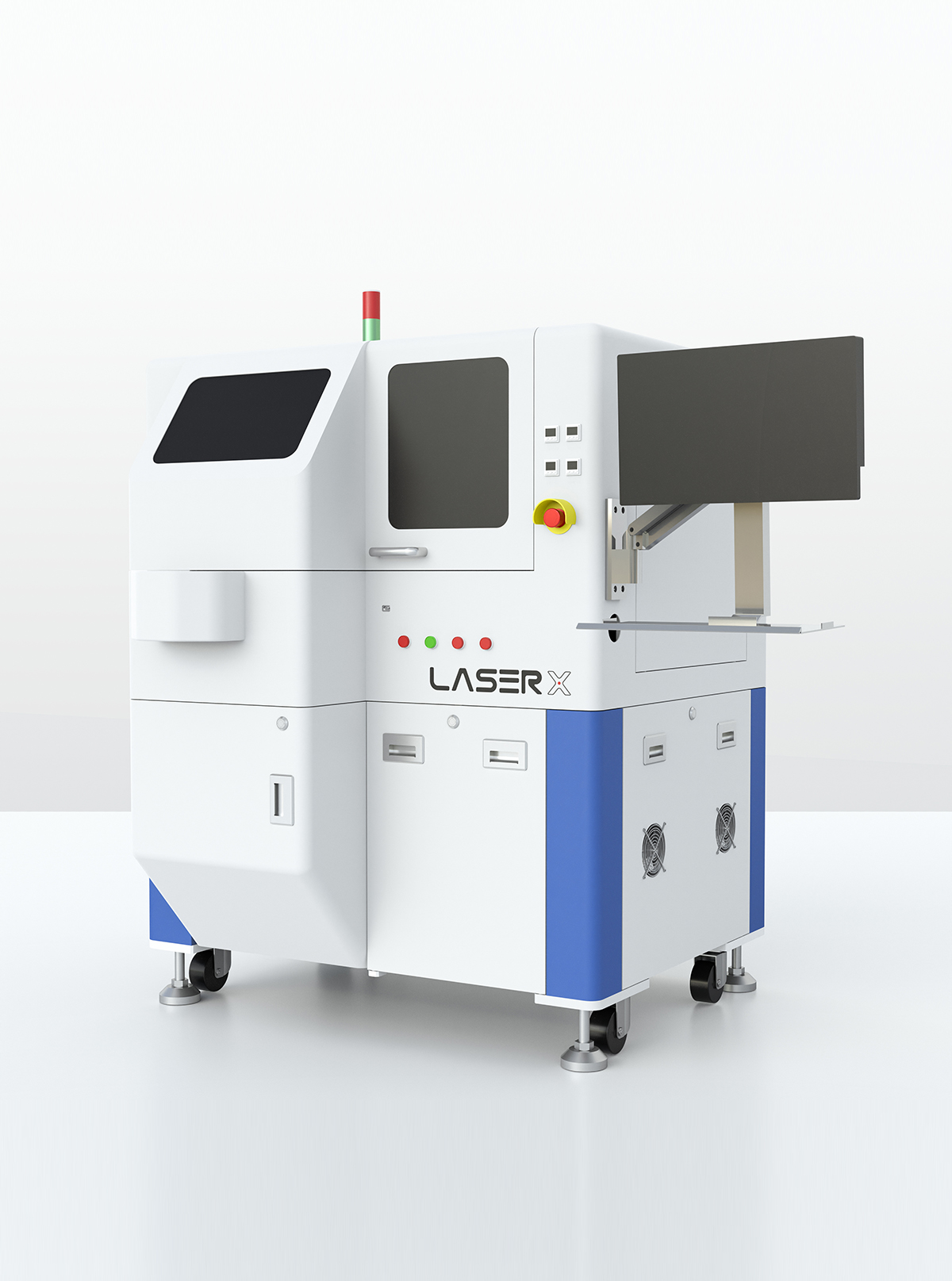
Designed for optical module/ lidar/ sensor/ SIP/ MEMS, etc., XY placement accuracy ± 3~5um@3σ
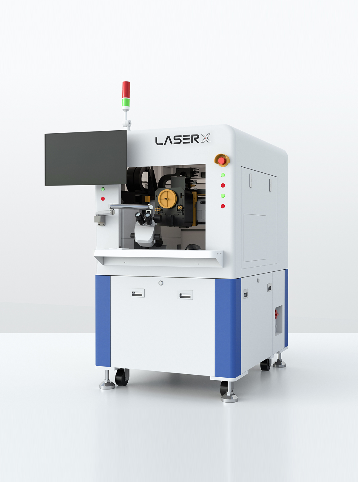
• Multi-chip bonding capability
- Auto bond-tool change, up to 4 bond-tool buffers
- Auto wafer change, up to 4 x 6” wafer ring
- Optional: Waffle pack, Gel-Pak, tray or by request
• Achieving ±3um XY placement accuracy
• Supports epoxy stamping and dispensing
• Automatic material handling system
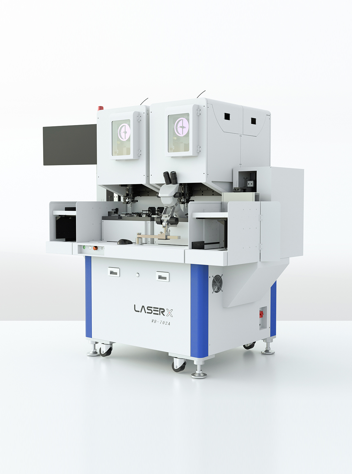
• Dual bonding head for higher production efficiency
• Stable bonding force control improve bonding quality and reliability
• Programmable ultrasonic power at different stages
• Real-time bond line length detection
• Tension detection to ensure product quality
• Quickly change of ribbon wire, aluminum wire
• Long gantry XY axis for large working area
• Bond quality control and assessment
• Direct drive linear motor and flying vision systems improve efficiency
• Quickly change of ultrasonic bond head supports aluminum wire, aluminum ribbon and copper wire bonding
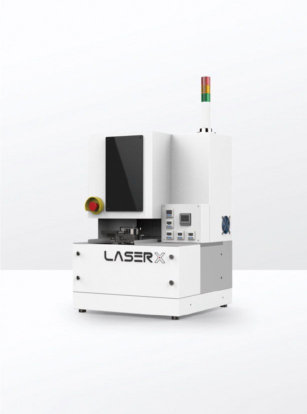
• Placement accuracy of ± 1.5 μm(3σ)
• Ability to handle tiny chips
• Apply LD and Submount cocrystal welding

 Shenzhen Headquarters:Building 3, Yufengda Industrial Park, Guangming District, Shenzhen City, Guangdong Province,518107 China
 Reception Service Number:0755-23019639
 Consultation Email:hongbin.ding@laserx.net & laserx.xs@laserx.net
About LaserxCompany ProfileDevelopment HistoryCompany CultureHonor and Qualification
ProductsBurn-in And TesterOptical AlignmentSemiconductor PackagingChip TesterHigh precision linear and goniometer slide
SolutionSmart Factory SolutionPhotonic Assembly and AlignmentIndustrial Laser Burn-in And TesterAdvanced packaging
Copyright © 2017-2026 LASER X Technology (Shenzhen) Co., Ltd. 粤ICP备2020137519号-1