Semiconductor Packaging
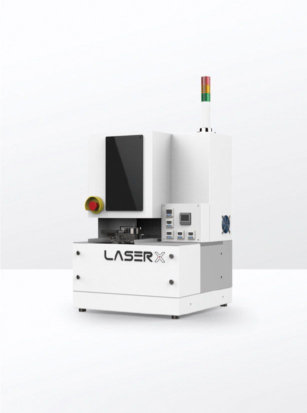
Semi-auto Eutectic Die bonder
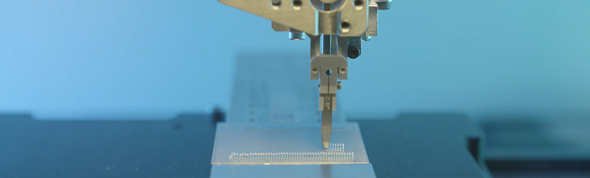
Product Feature
• Placement accuracy of ± 1.5 μm(3σ)
• Ability to handle tiny chips
• Apply LD and Submount cocrystal welding
 Download
• Placement accuracy of ± 1.5 μm(3σ)
• Ability to handle tiny chips
• Apply LD and Submount cocrystal welding
Download


 Shenzhen Headquarters:Building 3, Yufengda Industrial Park, Guangming District, Shenzhen City, Guangdong Province,518107 China
 Reception Service Number:0755-23019639
 Consultation Email:hongbin.ding@laserx.net & laserx.xs@laserx.net
About LaserxCompany ProfileDevelopment HistoryCompany CultureHonor and Qualification
ProductsBurn-in And TesterOptical AlignmentSemiconductor PackagingChip TesterHigh precision linear and goniometer slide
SolutionSmart Factory SolutionPhotonic Assembly and AlignmentIndustrial Laser Burn-in And TesterAdvanced packaging
Copyright © 2017-2026 LASER X Technology (Shenzhen) Co., Ltd. 粤ICP备2020137519号-1